研究テーマ / Research
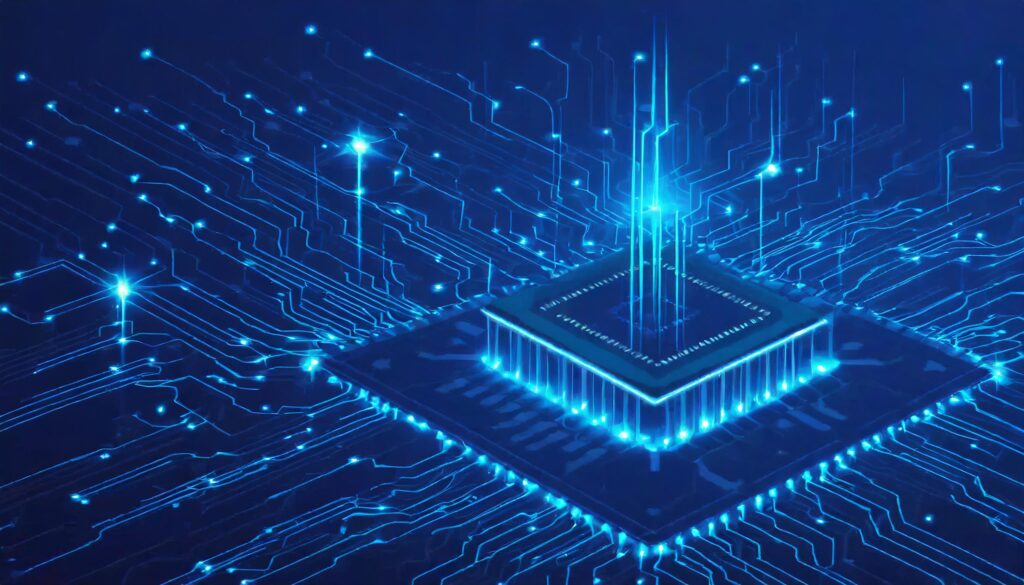
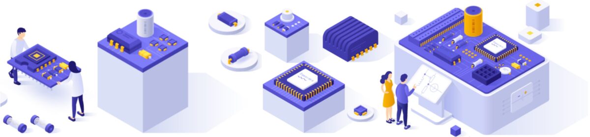
本研究室では次世代半導体レーザーを中心に、最先端の半導体デバイス・プロセスの研究を行います。より具体的には(1)メガワット級の高出力半導体レーザーを実現する新構造の提案・実証、(2)フルカラー色可変レーザーの実現、(3)光ピンセットを可能にするレーザーの超小型化・集積化、(4)nA級超低消費電力レーザーの実現などの研究を行います。いずれもこれまでにないアプローチで挑み、nature級を志向した野心的な研究とすることを目指しています。具体的な内容はResearchのページをご覧ください。
Our laboratory advances research into cutting-edge semiconductor devices and processes, with a focus on next-generation semiconductor lasers. More specifically, we will (1) propose and demonstrate a new structure that will realize megawatt-class high-power semiconductor lasers, (2) realize nA-class ultra-low power consumption lasers, and (3) develop tiny lasers that will enable optical tweezers. We also will (4) realize Full-Color Tunable Lasers. Each of these are ambitious research aimed at nature-level impact, taking on unprecedented approaches. Please see the Research page for more details.
教育方針 / Education

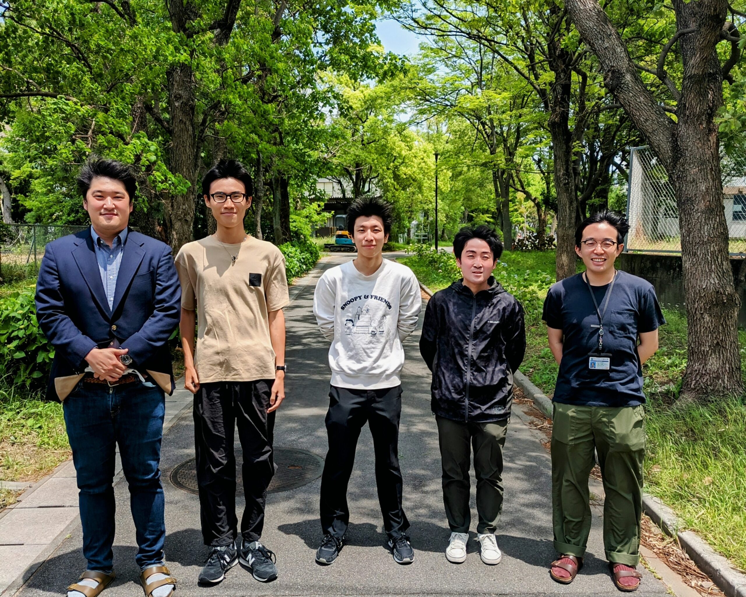
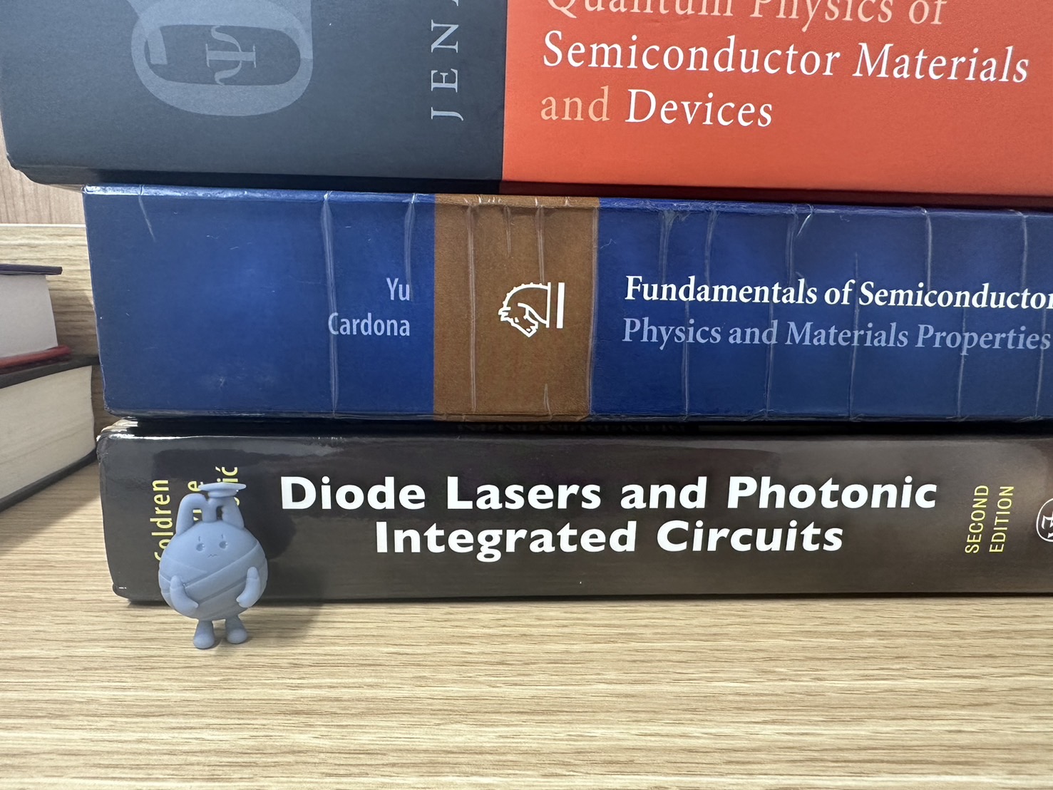
本研究室は、2024年まで大手半導体メーカーにて上席研究員を務めた企業出身者がPIを担当することに加えて、国内外のトップ研究機関出身の研究者が所属(予定)するなど、多種多様でハイレベルな人材が研究と教育を牽引します。指導スタッフの年齢層は全体として若めで、カジュアルな雰囲気で研究に取り組んでいただけるかと思います(詳しくはMembersをご覧ください)。配属された学生さんには、半導体デイバイスの動作原理や作製プロセスを学びながら、答えのない課題に挑む戦略的思考力、論理的コミュニケーション、チャレンジを楽しむメンタリティなど、企業に就職してからも役に立つ経験を積んでいただこうと思っております。
This laboratory has a wide variety of people, including the PI from a company who served as a senior scientist at a major semiconductor manufacturer until 2024, and researchers from top research institutions in Japan and overseas (TBD). High-level staff members will lead research and education. They are generally young in age, and thought to deliver a homely atmosphere (please see Members for details). The assigned students will learn the operating principles and manufacturing processes of semiconductor devices, while gaining experience that will be useful even when they enter companies after graduation, such as strategic thinking skills to tackle unanswerable problems, logical communication, and a mentality that enjoys challenges.
研究室の環境 / Environment

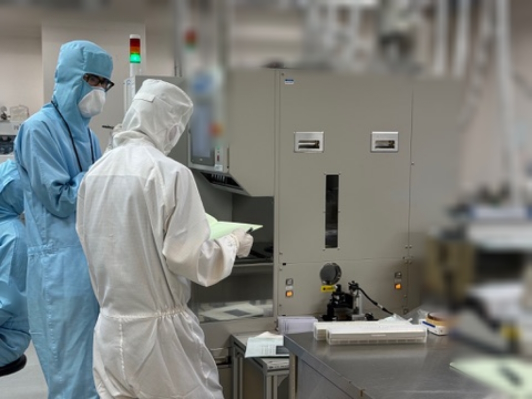
本研究室は半導体・デジタル未来創造センターの1組織ですが、学内の工学研究科をはじめとした学内組織と強い連携のもとにあります。例えば半導体デジタル未来創造センター姚研究室や、みえ未来図共創機構の中村(孝)グループなどと装置・研究ノウハウを共有しており、充実した環境のもと研究を推進することができます。また、日本国内・海外の組織との共同研究を通して、世界トップレベルの研究を遂行できる体制が整っています。
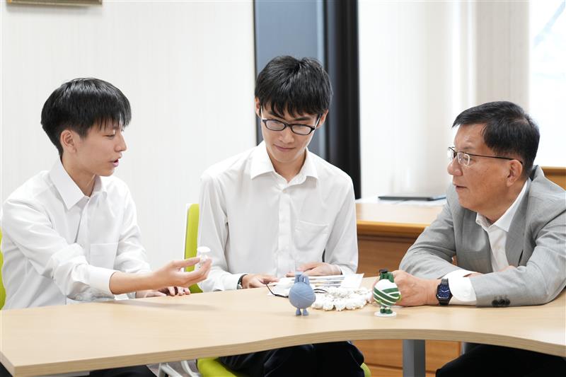
本研究室は地域イノベーション研究開発拠点に所在します。同棟は比較的新しく綺麗な建物です。また、学生の居室をはじめとした居住エリアはインテリアデザイナー監修のもとレイアウトされており、居心地の良い場所を大学生活の拠点として得ることができます。また、第一食堂を中心とした厚生エリアにもほど近い場所にあります。
半導体・デジタル未来創造センターについての詳細はICSDFutureをご覧ください。
This laboratory is part of Innovation Center for Semiconductor and Digital Future, and it also has strong collaboration with other organizations within the university, including the Graduate School of Engineering. For example, we can share equipment and research know-how with the Miyake group of the Optoelectronics Laboratory of the Department of Electrical and Electronic Engineering and the Nakamura (Takashi) group of the Mie Miraizu Co-Creation Institute, and promote research in a rich environment. . Additionally, through joint research with organizations in Japan and overseas, we have established an eco-system that allows us to conduct world-class research.
This laboratory is located at the Regional Innovation Research and Development Center. The building is relatively new and clean. In addition, the living areas including student rooms are laid out under the supervision of an interior designer, allowing students to have a comfortable place as their base for campous life.
For details about the Innovation Center for Semiconductor and Digital Future, please visit ICSDFuture.